Teardown shows Apple Watch S1 chip has custom CPU, 512MB RAM, 8GB storage
 Roger Fingas
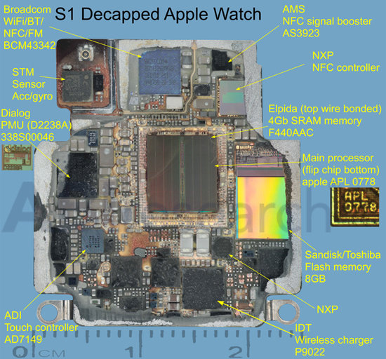
The first complete teardown of the S1 system-on-chip in the Apple Watch shows parts from a number of different manufacturers, including a Broadcom wireless chip, and memory from Elpida, Toshiba, and SanDisk, a detailed look inside the custom chip revealed on Thursday.
At the heart of the S1 is an Apple-designed processor, labeled the APL 0778, as discovered by ABI Research. The Broadcom chip is a BCM43342, capable of Wi-Fi, Bluetooth, NFC, and even FM radio, although the FM functions aren't actually used. Supporting the NFC capabilities, used for Apple Pay, are an NXP-made controller and a signal booster from AMS.
The device has 512 megabytes of Elpida RAM, which is paired with 8 gigabytes of storage from SanDisk and Toshiba. The Watch stores relatively little on-board, instead pulling most data from a paired iPhone. Users can, however, save a music playlist to their Watch for unpaired listening, and native third-party apps are planned for later this year.
Accelerometer and gyroscope functions are handled by an STM chip, while an ADI controller handles touch gestures. Finally, power is routed through a Dialog power management unit and an IDT-made wireless charger.
ABI commented that the S1 is an "obvious variation from Apple's smartphones," compressing many parts normally reserved for those devices. A recent Chipworks X-ray of the S1 showed that the STM chip is the first in an Apple product that merges accelerometer and gyroscope functions.


 Christine McKee
 William Gallagher
 Malcolm Owen
 Marko Zivkovic
 William Gallagher and Mike Wuerthele

 Wesley Hilliard
 Andrew Orr