Infrared microscope inspection of Apple's new A5X processor revealed that the chip was designed and built around Samsung's 45nm low power architecture, which is currently used in A5 processor found in the iPhone 4S and iPad 2.
As part of its comprehensive component-by-component analysis of the third-generation iPad, Chipworks has discovered that Apple's new A5X processor is being manufactured using Samsung 45nm CMOS process.
Measurements of the connected gates taken during cross-section analysis of the A5X confirm that it is a 45nm chip, similar in architecture to Apple's previous generation A4 and A5 silicon.
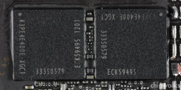
Unlike the older A-series chips, which sport a package-on-package design with the processing unit stacked below the LP-DDR2 SDRAM, the A5X configuration moves the 1GB of physical memory to a motherboard location opposite the processor.
Apple is continuing to source its memory from different suppliers as the Chipworks A5X used Samsung LP-DDR2, while an identical unit analyzed by iFixit implemented Elpida SDRAM.

Discrete DDR2 RAM modules, in this case Samsung-sourced. | Source: Chipworks
The A5X's die measures 12.82mm-by-12.71mm, which is a 35 percent increase in area compared to the A5 chip's 10.01mm-by-11.92mm die. Contributing to the increase in size is the addition of a quad-core GPU to the existing dual-core CPU.
Apple's new A5X chip boasts a 45nm LP CMOS architecture. | Source: Chipworks
Despite sharing the same CPU clock speed with the older A5 chip, the graphics and memory boosts in the new iPad's A5X processor should allow higher performance in graphics-intensive applications.


