The U.S. Patent and Trademark Office on Thursday published one of the first AuthenTec patent applications assigned to Apple, with the property describing an advanced method of fingerprint identification that can be embedded into a mobile device's display.

Source: USPTO
Apple's sensor patent details a technology that can not only fit into a mobile device like an iPhone, but can "read" biometric characteristics of a finger from distances larger than existing methods afford. The application, titled "Finger sensor having pixel sensing circuitry for coupling electrodes and pixel sensing traces and related methods," credits AuthenTec co-founder Dale R. Setlak as its inventor.
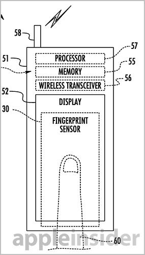
Current rumors and speculation point to a next-generation iPhone with fingerprint sensor built into the home button. If the technology outlined in Thursday's application is used, however, the sensor may instead be embedded in the iPhone's display.
The patent language notes the fingerprint sensor can be stacked with, or part of, an LCD display. As such, the sensor can also be used as a means of input, and can also be used in conjunction with other circuitry to support selection function, provide tactile feedback, or power up a device. Of note, the document points out that the sensor array can be either rigid or flexible, meaning mounting options are vast.

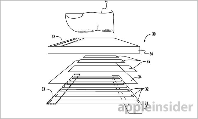
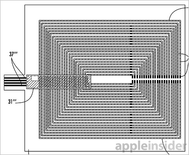
Key to the invention are pixel sensing traces coupled to the fingerprint sensor chip, which extend outward to form a first "metallization layer." These traces can be disposed in a variety of pixel sensing traces, as well as columns and rows of pixels, to form the required array. Certain embodiments support multiple sensors or staggered arrangements of sensing pixels depending on the application.
Sitting on top of the sensing traces is a dielectric substrate, which carries drive-or-shield electrodes that create a second metallization layer. In this setup, the structure of the pixel sensing traces below the substrate are insulated from the drive/shield electrodes, which are shorter in length than the traces. This arrangement allows the pixel sensing traces to extend beyond the electrodes, thus defining the finger sensing area.

Covering the sensing and drive/shield electrode substrate is another insulating layer that sits between the array and a user's finger. As noted in the document, this layer can be "the structural base of the fingerprint sensor."
In operation, the fingerprint sensor works by measuring electrical flux. A first switch couples a drive/shield electrode to touch screen circuitry, a finger drive source, and the voltage reference, while a second switch couples a pixel sensing trace to the field flux sensing component and the voltage reference. Sensing pixels are put into an activate measurement mode, while the electrodes sitting above are switched to a shield mode. Electrodes not situated above activated pixel traces are put into a finger drive mode, thus coupling it to the user's finger. As the pixel traces are scanned, the electrodes are switched between drive and shield modes, with flux measured against the reference voltage.
Finger sensor circuit diagram showing sensing traces (33), drive/shield electrodes (35) and switches (42, 43).
When not being used for fingerprinting purposes, the drive/shield electrodes can also be incorporated into touchscreen operations.
The patent application goes on to detail various methods of achieving low electrical crosstalk, minimizing parasitic capacitance, and other techniques that afford efficient functionality.
First filed for in January 2013 with a copending application from 2012, Setlak's invention makes mention of other AuthenTec properties as prior art. According to his LinkedIn profile page, Setlak is now an engineer for Apple in the company's offices in Melbourne, Florida.
Apple acquired the fingerprint sensor maker in 2012 for $356 million, fanning the flames of an iOS device using the firm's technology.