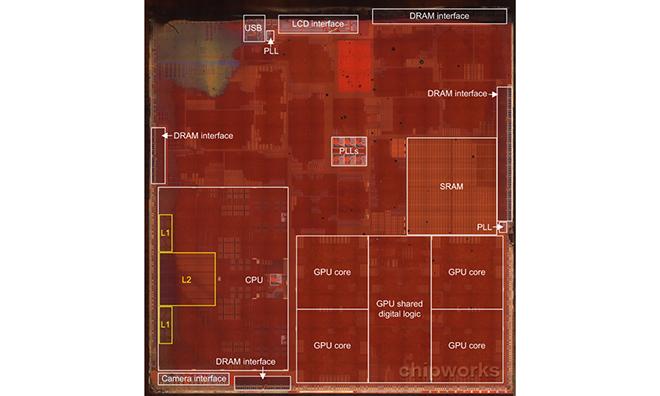
The team at Chipworks on Friday posted a tentative look at the iPhone 5s' A7 system-on-a-chip, finding a few changes from the previous A6 processor, including the addition of a mysterious SRAM cell never seen in A-series silicon.

Source: Chipworks
Continuing its comprehensive investigation of the new A7 SoC, which on Tuesday confirmed a 28nm manufacturing process, silicon experts at Chipworks are digging deeper into the processor's major structures and overall design.
The firm notes in the report that the latest findings are currently just "best guesses," as circuit extraction testing has not yet been performed to yield conclusive data.
Taking the caveat into consideration, one of the more interesting findings would be the "secure enclave" used for Touch ID fingerprint data storage that Apple discussed during the iPhone 5s reveal earlier this month.
Chipworks was unable to identify the area in today's image, however, but guesses that a new SRAM cell located above the GPUs is a prime suspect as the rather large storage space is a new addition to the A-series lineup. Extrapolating the size of the memory block and comparing it with metrics of known technology, the firm estimates the SRAM module to have a density of about 3MB.
Moving to the CPU, the A7's dual-core unit and accompanying memory, estimated at 1MB for L2 cache and 256KB for L1, takes up about 17 percent of the die area. Located across from the CPU setup is a quad-core GPU with shared logic, which accounts for 22 percent of on-die space.
A side-by-side comparison of the A7 and last year's A6 show the chips' CPUs do not share the same layout. The new A7 appears to be closer to a conventional automated design, which would be a departure from Apple's most recent custom-architected A-series SoCs.
Aside from the above discoveries, the rest of the A7's design appears to be carried over from the A6. Of note, the USB, LCD and camera interfaces are identical to those found in Apple's A5, A6 and A6X chips.

-xl-s.jpg)
