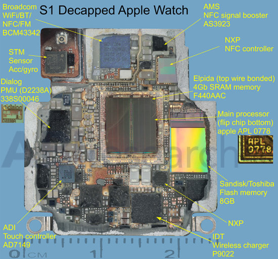
The first complete teardown of the S1 system-on-chip in the Apple Watch shows parts from a number of different manufacturers, including a Broadcom wireless chip, and memory from Elpida, Toshiba, and SanDisk, a detailed look inside the custom chip revealed on Thursday.

At the heart of the S1 is an Apple-designed processor, labeled the APL 0778, as discovered by ABI Research. The Broadcom chip is a BCM43342, capable of Wi-Fi, Bluetooth, NFC, and even FM radio, although the FM functions aren't actually used. Supporting the NFC capabilities, used for Apple Pay, are an NXP-made controller and a signal booster from AMS.
The device has 512 megabytes of Elpida RAM, which is paired with 8 gigabytes of storage from SanDisk and Toshiba. The Watch stores relatively little on-board, instead pulling most data from a paired iPhone. Users can, however, save a music playlist to their Watch for unpaired listening, and native third-party apps are planned for later this year.
Accelerometer and gyroscope functions are handled by an STM chip, while an ADI controller handles touch gestures. Finally, power is routed through a Dialog power management unit and an IDT-made wireless charger.
ABI commented that the S1 is an "obvious variation from Apple's smartphones," compressing many parts normally reserved for those devices. A recent Chipworks X-ray of the S1 showed that the STM chip is the first in an Apple product that merges accelerometer and gyroscope functions.

