As has become typical of every major Apple product launch, the new iPhone 5s is being torn down just hours after it officially went on sale in Australia, offering some of the first looks at the phone's innards.
Editor's note: This article was continuously updated as the teardown was in progress.
The techs at iFixit are in the midst of carrying out a teardown of Apple's latest flagship smartphone, which is expected to reveal unannounced specifications and internal layout.
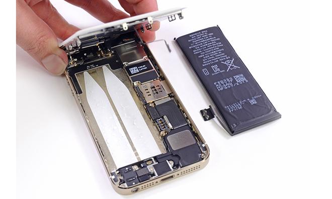
This year, the repair firm is tearing down the device live. So far, not much has been revealed aside from the battery, which is a 3.8V 5.92Whr unit, up from 5.45Whr in the iPhone 5.
The new iPhone's logic board appears to have been revamped, with enhancements including repositioned antenna connection placement that does away with cumbersome flex cables. The EMI shielding is also of note, as there are perforations for better cooling.
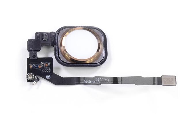
In conclusion, iFixit found no substantial changes to the iPhone 5s' internals compared to the iPhone 5. Aside from the slightly larger A7 SoC and Touch ID, the design is as expected. Interestingly, no mention was made of Apple's M7 motion coprocessor. Further investigation will likely reveal the chip's placement on the logic board.


