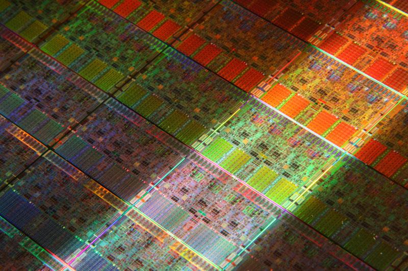
Intel this week offered its first official overview Nehalem, the highly scalable microarchitecture positioned to succeed Penryn in delivering a new generation of processors for notebooks, desktops, and servers, that offer "dramatic" energy efficiency and performance improvements.
The leap in performance and energy efficiency offered by Nehalem will be similar to the jump made by Intel's Core microarchitecture over the first 90-nanometer (nm) Pentium M processors, according to company vice president Pat Gelsinger. Key to this, he said, is simultaneous multithreading (SMT), an advanced version of hyper-threading that will create a new dimension in parallelism by enabling a single processor core to run two threads at the same time.
With Intel's plans for Nehalem calling for chips with 1 to 8 (or more) cores, this means a quad-core processor could run eight threads simultaneously, and similarly, an octo-core version up to sixteen threads simultaneously. Depending on the application, the resulting performance boost over today's Penryn chips could be as much as 20 to 30 percent, according to the chipmaker. At the same time, the ability to run more instructions in a single clock cycle allows the processor to return to a low-power state more quickly, therefore also boosting power efficiency.
Nehalem processors will also utilize a new point-to-point processor interconnect called Intel QuickPath Interconnect, which will serve as a replacement for the legacy front side bus (FSB). Instead of using a single shared pool of memory connected to all the processors in a server or high-end workstation through FSBs and memory controller hubs, most Nehalem processors will pack their own dedicated memory that will be accessible directly through an Integrated Memory Controller on the processor die itself.
In cases where a processor needs to access the dedicated memory of another processor in a multi-processor system, it can do so through the QuickPath interconnect that links all the processors. This improves scalability and eliminates the competition between processors for bus bandwidth, according to Gelsinger, as there is no longer a single bus for which multiple chips would need to contend in order to reach memory and I/O services.
Nehalem will also offer the option for an integrated graphics controller for highly efficient mobile designs, and add an inclusive shared L3 (last-level) cache that can be up to 8MB in size. In addition to being shared across all cores, the L3 cache can increase system performance while reducing traffic to the processor cores.
Other features discussed by Gelsinger during this week's Nehalem architectural briefing include support for DDR3-800, 1066, and 1333 memory, SSE4.2 instructions, 32KB instruction cache, 32KB Data Cache, 256K L2 data and instruction low-latency cache per core and new 2-level TLB (Translation Lookaside Buffer) hierarchy.
The majority of these advancements are pertinent to Apple, as the company's ongoing Mac roadmap implies that it will at the very least adopt both server and mobile variants of Nehalem, beginning with a Xeon-based successor to the Harpertown chip presently powering its Mac Pro line of professional desktop systems.


