Apple has quickly moved to overhaul the equipment installed at the San Jose, Calif., chip fab it acquired from Maxim Integrated Products in December, indicating that the purchase was a strategic priority for the company in its relentless drive to out-innovate its competitors.
The relatively small 70,000-square-foot silicon chip fab, reportedly referred to internally as "Athena," the Greek goddess of wisdom and warfare, had previously served as a low volume manufacturing facility for Maxim Integrated Products, supporting process technology development.
What will Athena do with her delicate equipment?
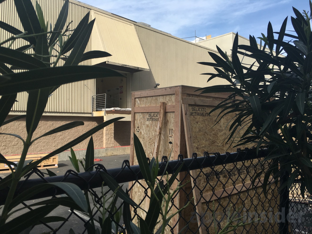
Apple rapidly initiated efforts to retrofit the equipment installed at the former Maxim fab shortly after taking possession of the facility. Semi trailer truckloads of equipment, wrapped in anti-static foil (below) labeled as "delicate instruments" have been unloaded at at the facility for installation, indicating that the building wasn't just acquired as a curiosity to dabble in rudimentary chip experiments.
At the same time, Apple's current and expanding relationship with TSMC makes it clear that the Athena facility isn't ever going to take over the extremely sophisticated role of building Apple's world leading, advanced A-series Application Processors that power everything from Apple TV to iPhones to the new iPad Pro, nor the S-series System-in-Package component that runs Apple Watch.
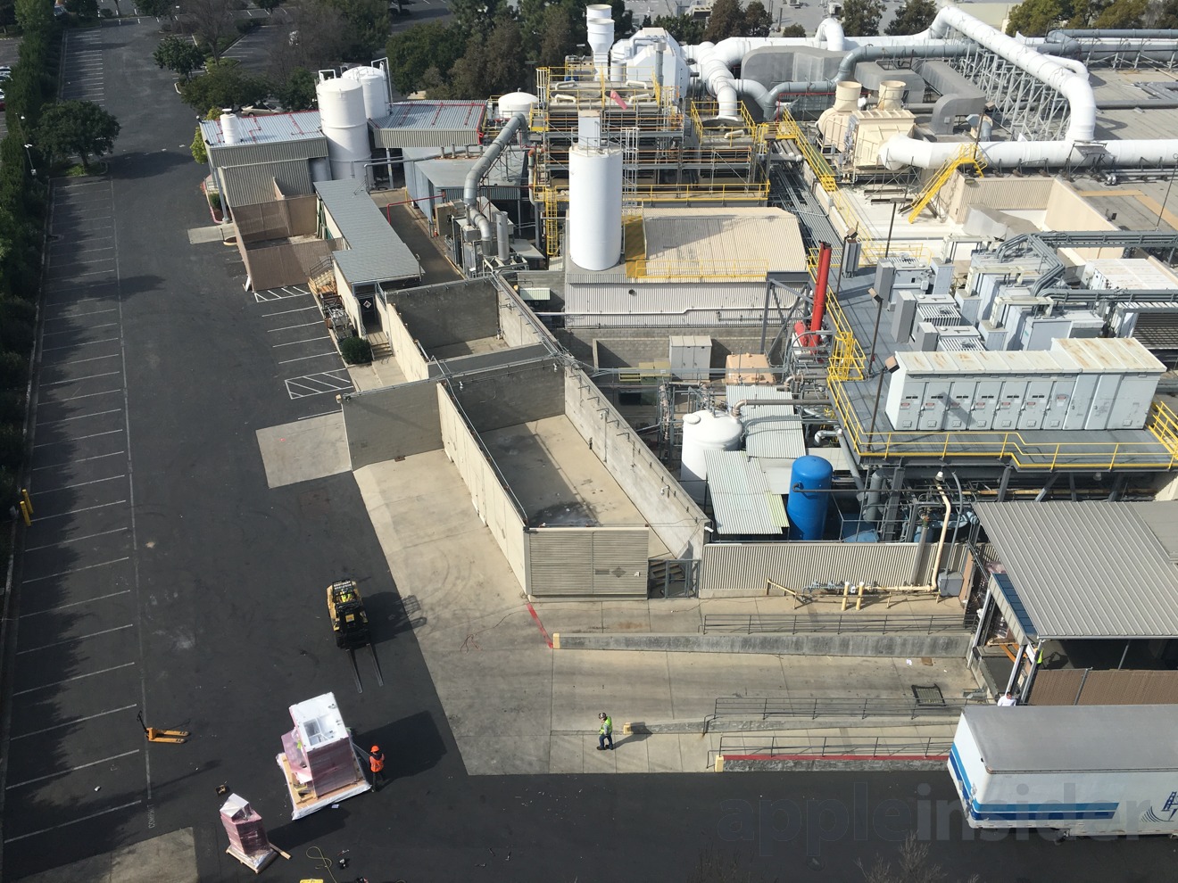
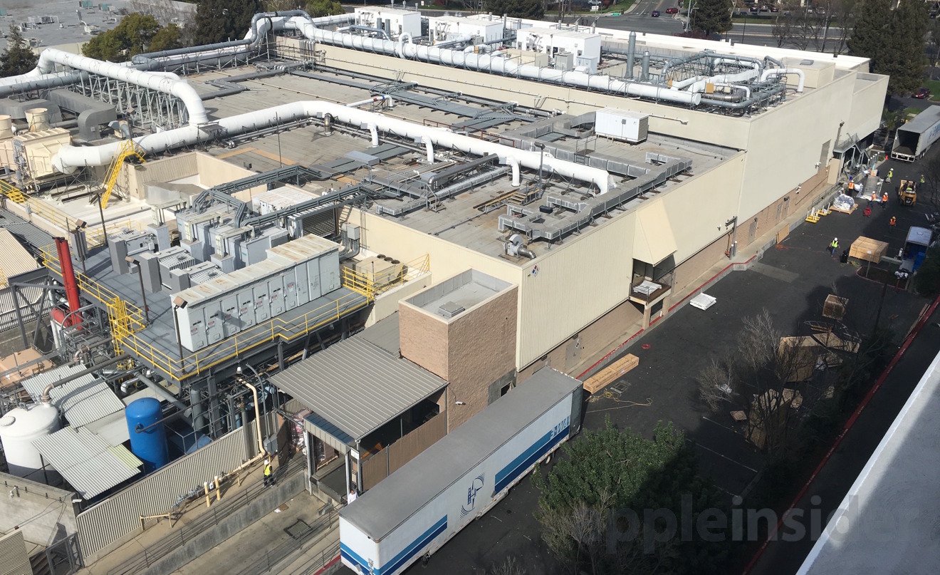
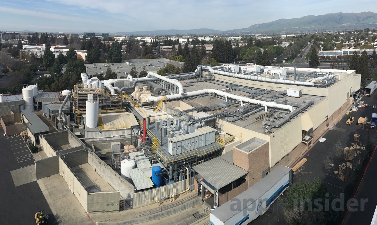
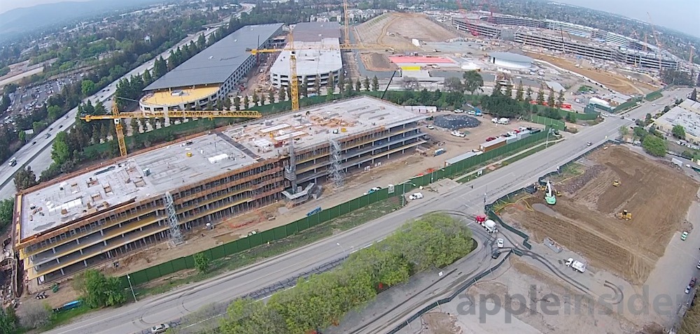
The size and location of the Athena facility also makes that clear; there's no real potential or rationale for shifting existing, high-end chip production to it. It also makes no sense to convert the building to basic office space, as the facility is specialized to accommodate the production of electronics devices, as is evident in the aerial images (below).
Apple has also acquired multiple large tracts of land, much of which is still undeveloped, that would offer far greater potential for building new office space or prototyping facilities, and the company has also leased a series of buildings offering immediate use office space or workshops scattered around Silicon Valley.
Apple also is in the process of completing an extremely large expansion of office space at the new Campus 2, which is expected to reach completion around the end of this year. Additionally, a very large new series of workshops and testing facilities, along with a dedicated data center installation, is also being built in parallel as part of the Campus 2, Phase 2 project (below). That entire development is located just a few minutes away from Apple's existing Infinite Loop Campus in Cupertino, California.
All of these other developments currently in progress indicate that Apple actually acquired the Maxim chip fab (located relatively far away from its headquarters and other offices, in a more industrial, silicon manufacturing corridor) explicitly to gain silicon chip fabrication capacity.
Maxim used the lab for MEMS production
Maxim had originally been using the fab to produce micro-electro-mechanical system sensors ("MEMS," micro machine components printed like silicon logic chips) targeting the consumer market. The company announced a departure from the market last year, reportedly after losing a contract to supply components to Samsung for use in a flagship smartphone.
MEMS components include tiny devices like accelerometers and gyroscopes (both for sensing motion), pressure sensors (like the barometer included in iPhone 6/6s models), projector displays using DLP technology, IMOD or interferometric modulator displays, and medical devices that can monitor things like blood pressure or detect chemicals.
After being shut down by Maxim last summer, the facility was initially shopped around as being "well suited for prototype, pilot, and low-volume manufacturing."
A real estate listing noted: "this facility is capable of producing a wide array of products at multiple technology nodes ranging from 600nm to 90nm, with the bulk of production from 350nm to 180nm," and it described the property as including "a complete tool line consisting of 197 well-maintained front-end tools from such OEMs as AMAT, Hitachi, Novellus, LAM, TEL, KLA, and ASML."
Apple's modern Macs and iOS devices use chips manufactured by a broad range of partners, including Samsung, Intel, Broadcom, Texas Instruments and many others. These components typically require far more advanced process nodes than the acquired Maxim site was capable of delivering.
By way of comparison, the Samsung ARM chips used in the original iPhone and 3G were built using a 90nm process. Apple's latest iPhone 6s uses 14-16nm A9 chips, although other supporting chips are often manufactured with less advanced fab technology in order to save money. For example, last year's M8 motion coprocessor was manufactured at a 90nm process.
Various MEMS sensors used in iPhones and in Apple Watch could be fabricated in such a facility, but Apple already sources common parts from outside chip partners. Using Athena to develop a unique, proprietary new type of device would make sense, however. This could give Apple another multi year lead in offering a breakthrough new feature much the same way that its acquisition of Authentic enabled it to deploy Touch ID, and then Apple Pay, on new iPhones as a strong, differentiating and exclusive new feature.
With its own MEMS fab, Apple could also develop innovative new medical sensors for use in Apple Watch, such as a wearable blood pressure, blood oxygen, or blood sugar monitoring technology, offering a huge new boost in capability, while also supporting new kinds of clinical studies for ResearchKit, further expanding its audience.
Other technologies Apple could prototype, and possibly even build, at the Athena facility include advanced new wireless antennas for improving the reception and range of Bluetooth and WiFi across its entire product line, or energy induction devices for deploying real wireless power that doesn't require a device to physically contact with a wired charging device (as Apple Watch and many "wireless power" chargers currently use). This could convert Apple's AirPort basestations into wireless charging devices that keep mobile phones, wearables, keyboards, Siri Remote, Apple Pencil and other peripherals charged without requiring wires and adapters.
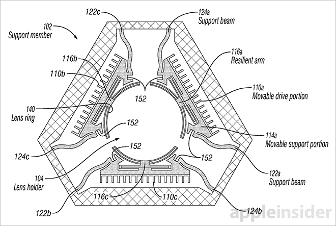
Apple has also previously documented interest in using MEMS components to provide camera lens autofocus (depicted above), and specialized, multiple MEMS microphones have already long been used in Apple's products to provide noise cancellation.
Whether Apple plans to use the Athena fab to make custom chips or other components for use in upcoming products, or to prototype new parts that will ultimately be manufactured by other partners, significant upgrades were apparently necessary. Whatever its plans for the facility are, the upgrades Apple is installing have been performed in public view of the site's adjacent neighboring facility recently built by Samsung.
 Daniel Eran Dilger



-m.jpg)






 Marko Zivkovic

 Mike Wuerthele
 Christine McKee
 Amber Neely
 Wesley Hilliard

 William Gallagher





19 Comments
I'm going with MEM for camera lens assemblies.
i'm going with manufacturing their own baseband chips; what better way to maintain security than to have a vertical through manufacturing.
"What will Athena do with her delicate equipment?"
Ok, that made me blush a little bit.
(maybe something to do with the company being named "Maxim"?) B)
I used to write circuit simulation software for Intel. I have no doubt that Apple will use this for development of new A10, A11, S2, S3, etc. chip designs. Daily chip design work is confirmed by simulation, but every month or so one needs to manufacture a small batch of actual silicon to validate the simulations. Without its own little fab such as this one, Apple would have to send their preliminary (and highly secret) designs to their chip manufacturing partners TSMC and Samsung. With its own little fab such as this one, Apple can use exactly the same equipment that TSMC and Samsung would use in production to validate their designs while keeping their design secrets (relatively) safe within Apple until they are ready to go into production.