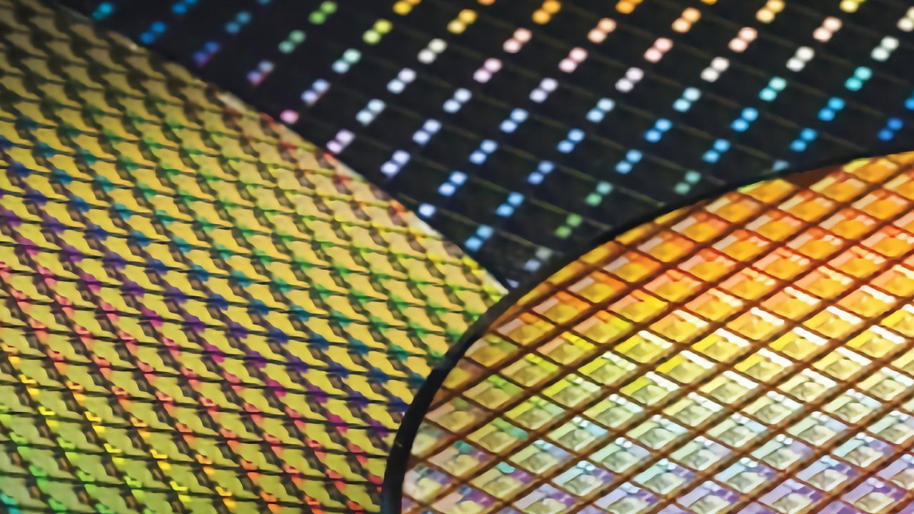
The A20 chip that will be used in the iPhone 18 could be packaged with a new tech that will give Apple more configuration options, while still being as small as possible.
Apple's chips, produced by TSMC, are currently packaged using a method known as InFo (Integrated Fan-Out), which helps create very compact chips for use in the iPhone. However, if a leaker is to be believed, Apple could switch to something different.
In a Weibo post by "Mobile Phone Chip Expert" on Monday, it is claimed that the A20 will be a 2-nanometer chip that uses a new packaging method known as WMCM. The leaker also adds that the memory will also be upgradedto 12GB for all models.
The change from the 3nm process used in the current-gen A18 chip to a 2-nanometer one should help reduce the size of the die, as well as cutting power consumption and helping with heat. The 12GB will also be an increase from the 8GB used in the iPhone 16 range.
However, the packaging change could be more beneficial for Apple's future plans.
Repackaging
Chip packaging refers to a process that is applied to a chip's die. One that sets it up to communicate and work with other components on a circuit board.
The current packaging technique, InFo, is useful for Apple as it enables for components to be integrated within the chip package. That means elements like memory can be added to the chip package directly, rather than being an externally accessed component.
This has the byproduct of making the overall chip package very small. However, it is a technique that also focuses on being used with a single die.
For Apple's current setup of including the CPU, GPU, and Neural Engine on a single die and then fitting memory on top, this works fine. But, if you wanted to include different combinations of CPUs and GPUs in the package, you would have to produce different dies, which can get expensive very quickly.
WMCM, also known as Wafer-level Multi-Chip Module, is a packaging technique that plays well with multiple dies. It can fit together separate dies, such as a CPU and GPU, while still keeping the overall package extremely small.
This is also done without massively sacrificing on performance, as the dies are so closely packed together.
For Apple, switching to WMCM provides more freedom to create multiple packaging designs by incorporating different dies. All without massively increasing the cost of creating the dies themselves.
It could potentially allow Apple to add extra bits to its Pro chips while leaving them out of the non-Pro variants. Doing so would mean the chips in the Pro and non-Pro iPhone could be made using the same technology generations, but without relying on chip binning to differentiate the two tiers.
There's also the possibility of incorporating the different elements together in various configurations. For example, vertically stacking some aspects while placing others next to each other on the same level.
A plausible upgrade
The source of the leak, "Mobile Phone Chip Expert," has a history of Apple chip pronouncements. In July, they said that Apple won't be using a 2nm process until the iPhone 18 Pro, in 2026.
They also said in June 2023 that the A18 would switch to an N3E process from N3B, which turned out to be correct.
While the leaker has a generally good reputation for accuracy, the claims are in a timeframe that could end up taking years to actually confirm.


