Teardown shows Apple Watch S1 chip has custom CPU, 512MB RAM, 8GB storage
 Roger Fingas
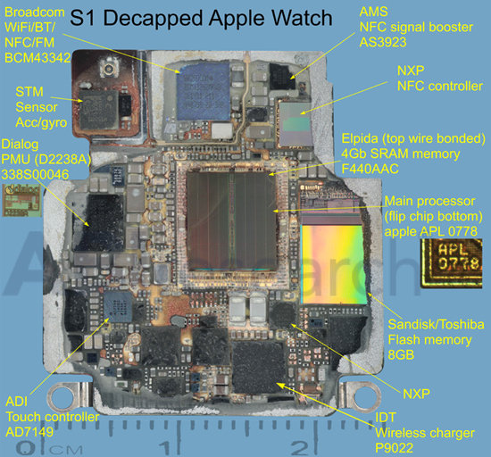
Last updated
The first complete teardown of the S1 system-on-chip in the Apple Watch shows parts from a number of different manufacturers, including a Broadcom wireless chip, and memory from Elpida, Toshiba, and SanDisk, a detailed look inside the custom chip revealed on Thursday.
At the heart of the S1 is an Apple-designed processor, labeled the APL 0778, as discovered by ABI Research. The Broadcom chip is a BCM43342, capable of Wi-Fi, Bluetooth, NFC, and even FM radio, although the FM functions aren't actually used. Supporting the NFC capabilities, used for Apple Pay, are an NXP-made controller and a signal booster from AMS.
The device has 512 megabytes of Elpida RAM, which is paired with 8 gigabytes of storage from SanDisk and Toshiba. The Watch stores relatively little on-board, instead pulling most data from a paired iPhone. Users can, however, save a music playlist to their Watch for unpaired listening, and native third-party apps are planned for later this year.
Accelerometer and gyroscope functions are handled by an STM chip, while an ADI controller handles touch gestures. Finally, power is routed through a Dialog power management unit and an IDT-made wireless charger.
ABI commented that the S1 is an "obvious variation from Apple's smartphones," compressing many parts normally reserved for those devices. A recent Chipworks X-ray of the S1 showed that the STM chip is the first in an Apple product that merges accelerometer and gyroscope functions.


 Amber Neely
 Thomas Sibilly
 AppleInsider Staff
 William Gallagher
 Malcolm Owen
 Christine McKee


32 Comments
In other words, more computing capacity than my original 2007 iPhone!
Unfathomable complexity and minuteness. The people who make these things may as well be gods.
[quote name="Suddenly Newton" url="/t/186068/teardown-shows-apple-watch-s1-chip-has-custom-cpu-512mb-ram-8gb-storage#post_2718295"]In other words, more computing capacity than my original 2007 iPhone![/quote] In others words, iPhone needs more RAM. :)
[quote name="pembroke" url="/t/186068/teardown-shows-apple-watch-s1-chip-has-custom-cpu-512mb-ram-8gb-storage#post_2718297"]Unfathomable complexity and minuteness. The people who make these things may as well be gods.[/quote] I'd like to see this crammed into a single chip. I'm amazed wifi fits in there, antenna and all. I remember trying to get a CF Card Wifi adapter to work with an old Sharp Zaurus Linux PDA and finding the PDA's battery life would go from "joke" to "why bother?"
Apple's on a roll on miniaturization. First the new MacBook with a complete, full featured computer (not part of it like the Intel stick) motherboard in 4x1.5 inches, then a remarkable Apple Watch S1 in less than 2x2 inches. For those complaining that it's performance doesn't match a Mac Pro, look at what Apple crammed into so little space. I would say the Apple Watch is as powerful as many cut-rate PCs of today and comparable to a regular Mac from the turn of the century. Think about the options Apple has in creating other devices using the S1 as the main building block. Get rid of the watch-only items and they've got a good computing platform that would fit almost anywhere. A typical automotive ECM could fit a dozen S1-based systems inside it's box.