Anandtech published a preliminary technical analysisa of the new iPad on Thursday based on iFixit's teardown of the device.
Report author Anand Lal Shimpi said the tablet's internals were "mostly what we expected," including the Qualcomm MDM9600 LTE baseband. However, working from images of the third-generation iPad's insides, he did surmise that Apple is now using "two discrete DRAM devices" for its A5 SoC, instead of a PoP (Package-on-Package) stack.
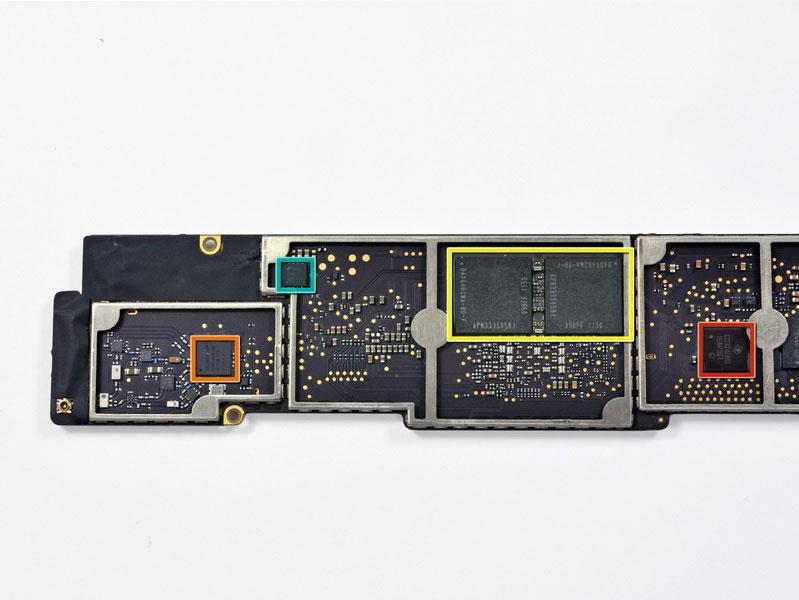
The two 512MB Elpida LP-DDR2 devices were located "on the side of the PCB that doesn't feature the A5X," he said. The DRAM devices carried a part number of B4064B2MA-8D-F, but Lal Shimpi was unable to identify detailed specifications by reading the part numbers.
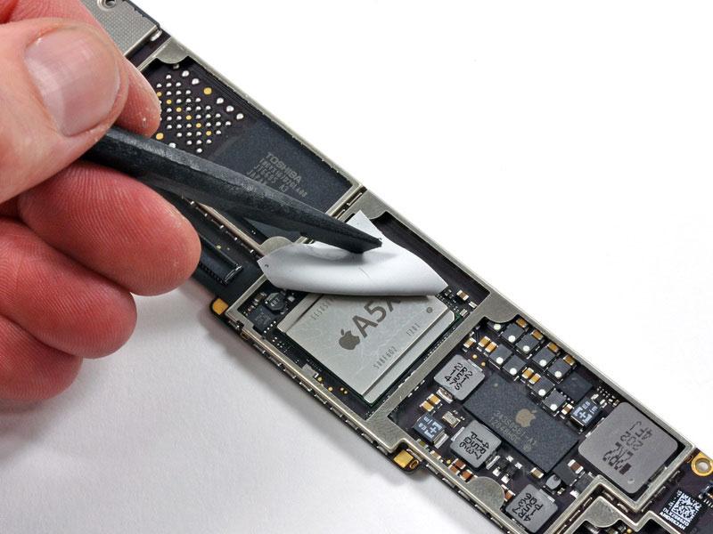
Another change reported by the publication was the addition of a metal heat spreader to the A5X. Lal Shimpi took the to mean that Apple had "made the shift from a wire bond package to flip-chip," the process of flipping a chip top face down to connect it to external circuitry.
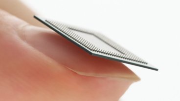
"Moving to a flip-chip BGA package allows for better removal of heat (the active logic is closer to the heatsink), as well as enabling more IO pins/balls on the package itself," he said.
However, Lal Shimpi did note that Apple may have already used flip-chip in the previous-generation A5 and "simply hidden it under the PoP stack."
The report went on to estimate the die size of the new A5X chip. By comparing Apple's new SoC with the Toshiba eMMC NAND next to it, Lal Shimpi deduced that the A5X die measured roughly 10.8mm x 10.8 mm, or 117.5mm^2. Anandtech had previously guessed a 125mm^2 die for the A5X. He assumed that the A5X is built on a 28/32nm process, but he also warned that there was "a lot of estimation" in his methodology.
Apple's new A5X has the same clock speed as its predecessor, but features double the RAM and a new quad-core graphics processor. According to iFixit's teardown, the CPU was built by Samsung and is believed to have been manufactured during the first week of 2012. Samsung also manufactured the Retina Display found in the new iPad used for the teardown.
The third-generation iPad launches in 10 countries at 8 a.m. local time on Friday, though some retailers began selling the device at midnight.


