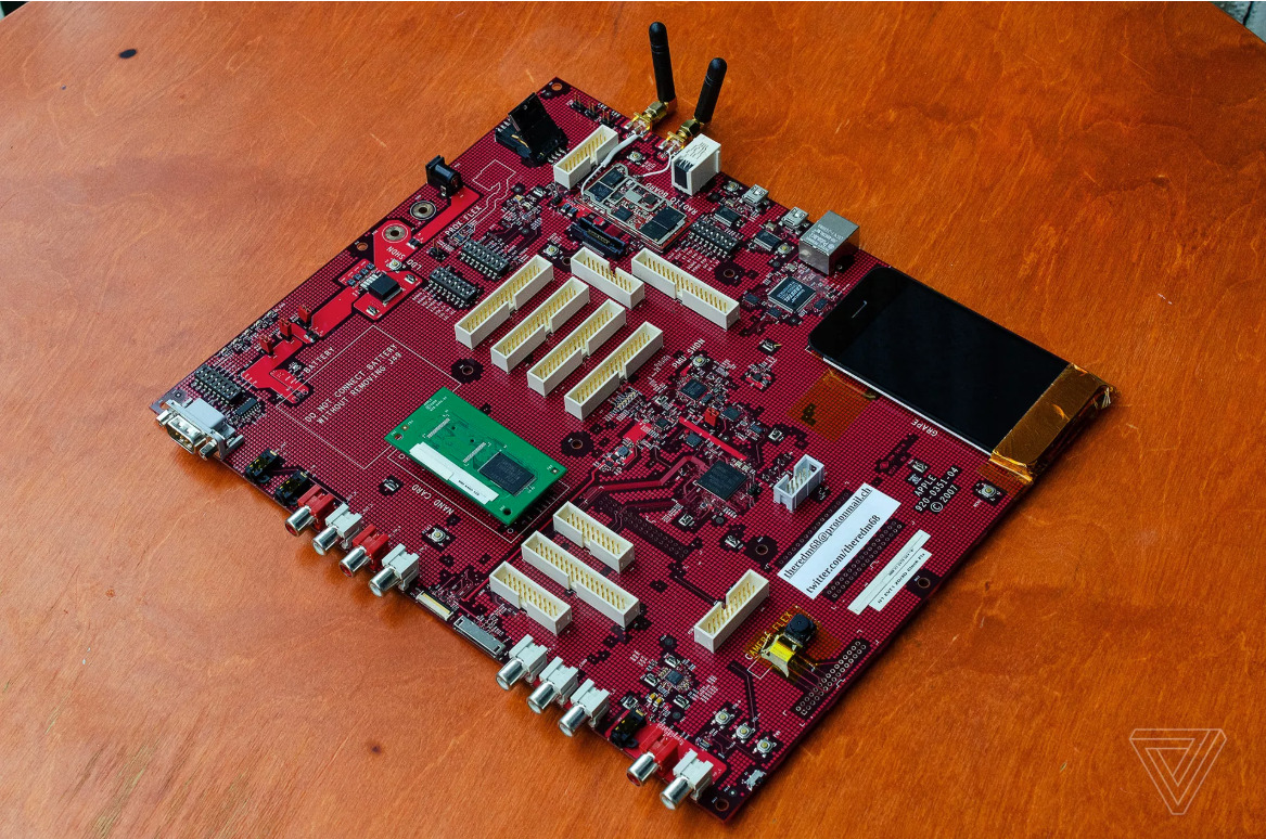
Photos have emerged of one of Apple's original development prototype boards for the 2007 iPhone, effectively detailing the device's exploded internals.
The unit was an engineering validation test (EVT) sample intended for staff working mostly on the iPhone's software and wireless technology, for instance porting the Darwin kernel over from Mac OS X, The Verge said. Those people wouldn't have been aware of the product's final form, and some versions of the board are said to have been without the depicted screen, requiring an external component or RCA display.
Many of the elements on the board represent parts that would eventually make their way into the final product, such as a 30-pin connector, a SIM card slot, and Wi-Fi and Bluetooth antennas. Others are unique, including an RJ11 phone jack for testing voice calls, and two mini USB connections for accessing processor and baseband chips.
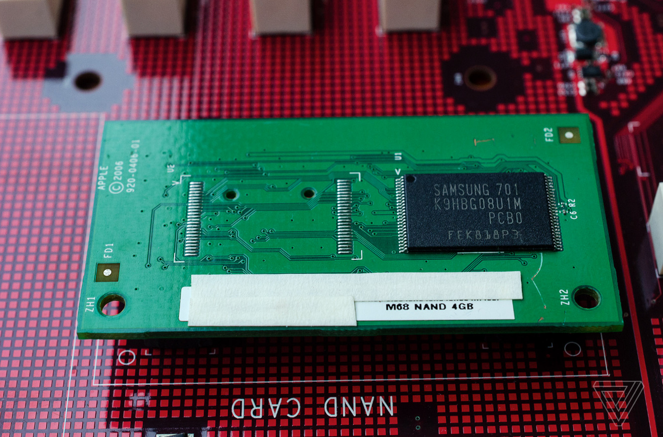
The application processor is a Samsung K4X1G153PC, combining Samsung memory with an ARM1176JZF to run iPhone OS. Also present is 4 gigabytes of Samsung NAND storage, removable in this case so that software changes can be tested by swapping cards.
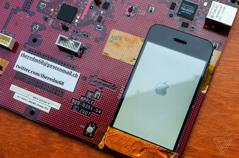
Despite appearances a home/menu button is actually situated to the left of the display. Power and volume buttons are also on the board, though trying to turn it on now simply brings up an Apple logo. During the iPhone's development in 2006 and 2007, engineers would have had deeper command access.
The exploded layout made it easier to debug and alter the prototype. DIP switches, for example, could route signals along different paths.
One unusual point is that if the board is connected to a modern computer, iTunes will detect it as an iPhone needing to be restored.
Apple ultimately launched the first-generation iPhone on June 29, 2007. The company is said to have moved on to smaller test boards for later models, in some cases integrating security shields to block prying eyes.
It turns out that I have a slightly better version of this iPhone prototype photo, plus two more from that same day, Feb 4, 2006. //cc @stroughtonsmith pic.twitter.com/DCOPyOFMUu
— Ken Kocienda (@kocienda) March 19, 2019
