As companies like Intel and TSMC plan future processors and chip designs that use extremely small scale production processes, AppleInsider takes a moment to explain what die shrinking is, how it can benefit everyone involved, and how it's now an extremely difficult feat to perform.
What is a die shrink, anyway?
A "Die Shrink" is the name given to when a chip fabricator changes the scale of production for the die, the circuitry made up of tiny transistors that modern processors are made from. As the "Shrink" part suggests, the circuits themselves are more compact, with smaller pathways and elements used in its creation.
By using a smaller process, a circuit could take up less space than it would usually occupy. This means there could be more space available for more circuitry to be laid down, increasing what the circuit could be capable of doing, and allowing for far more complicated circuits to be designed and produced.
It also benefits chip foundries in terms of cost, as shrinking the die means more comparable-complexity chips could be produced on the same wafer of silicon than earlier, bulkier processes. The more dies a company can fit onto a wafer, the lower the cost-per-chip of the wafer itself.
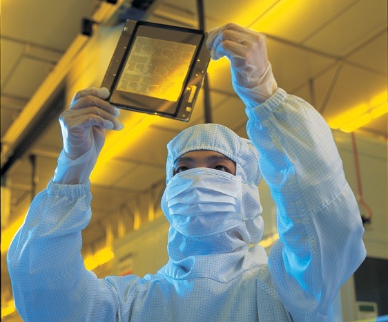
A TSMC worker in a clean room used for chip production (via Taiwan Semiconductor Manufacturing Co., Ltd.)
Aside from performance generated from more complex circuitry in a processor, there are other benefits to a die shrink that can be more relatable to consumers. Using a smaller process with less material means there is a reduction in the amount of power consumed compared against older processes, as well as lower heat generation that requires less cooling by heatsinks and fans.
The lower power and heat also opens up the opportunity of increasing the clock frequency, allowing for the circuit to be used more times in a period while maintaining a comparable amount of cooling, in turn raising performance.
There is also the opportunity for the cost savings associated with using less silicon for a chip to be passed on to device producers, and in turn consumers, though this generally benefits the hardware producer far more than the end user.
Ultimately, it is in the best interests of chip companies, device producers, and consumers for new fabrication processes to be created to make things smaller, and generally better for all involved.
On the level
Over the years, the process level used for each successive die shrink is set out by the International Technology Roadmap for Semiconductors (ITRS) which are guidelines created by assorted industry experts and sponsor companies. While not a strict ruleset, the documents offer just an assessment for what producers in the industry should consider when working towards the next step in die shrinking.
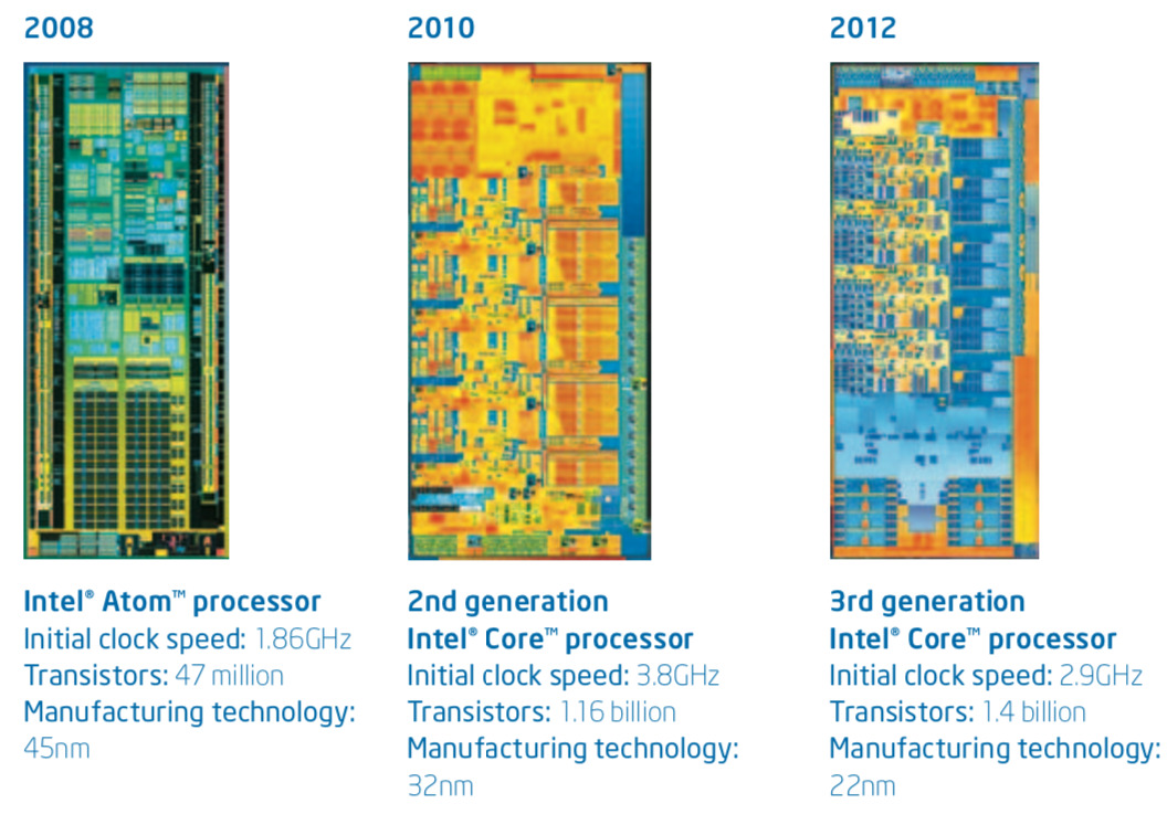
As the process shrinks, the designs get more complex as more transistors can be placed into a smaller space (via Intel)
This could be seen as a way to try and get the chip foundries onto the same page regarding processes, especially as many of the recommendations are provided for sizes that are years away from reaching commercialization. However, it is up to each company as to how each proceeds with the next generation.
Despite not having any power over how companies actually perform die shrinks, the roadmap has still helped to guide firms in deciding what the next die shrink level should be. The ITRS has defined the level of well-known process size levels as 65 nanometer, 45 nanometer, 32 nanometer, 14 nanometer, 10 nanometer, the 7-nanometer used in the current A-series chips, 5 nanometer, and even expects 3-nanometer processes to be in use by 2022.
Tick-Tock, Moore's Law won't stop
While not directly a die shrink, it is worth bringing up the concept of the "Tick-Tock" model of processor design. While a die shrink is widely agreed to be a way to improve a processor over time, it isn't the only method available to a chip producer, as they could get away with improving the design using existing processes.
In the case of the model, a "Tick" is a die shrink that improves performance using an existing design, referred to as a microarchitecture, bestowing upon it the benefits of the shrink without majorly altering how the design functions. The "Tock" is where alterations are made to the microarchitecture to improve overall performance.
The model relied on a steady swing between the die shrinks and the microarchitecture changes, with the cadence similar to that of a clock, giving the name.
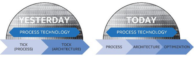
Intel's illustration of its extra 'tock' cadence strategy adding an optimization step between die shrinks
For quite a while, this was the norm, and allowed companies like Intel to continue to adhere to "Moore's Law," referring to a suggestion by former Intel CEO Gordon Moore that the number of components in an integrated circuit would double each year for at least a decade until 1975, before being revised to every two years. Effectively, this meant a potential doubling of performance, if the law could be adhered to long-term.
However, die shrinks to extremely small levels are becoming harder to process, with the laws of physics now interfering with attempts to go down to smaller process levels.
In 2016, Intel effectively gave up on trying to follow Moore's law, switching the cadence to one of "Tick-Tock-Tock." By optimizing the architecture improvements of the previous "Tock," this gave more of an opportunity to use the existing and already paid-off processes, while buying time to prepare for the next new "Tick."
Smaller, but not always
Even if a company states that a chip uses a specific level of nanometer for its production, the description may be true, but doesn't necessarily apply to the entire chip. The nanometer number references the smallest possible line that could be created using the process.
This does not however mean that all sections of a processor design use elements of that specific size. It is entirely possible for elements in a design to be made larger than would theoretically be allowed using the process level, such as parts of a design having issues working properly at a smaller scale.
In effect, a die shrink is like making a drawing using a narrower pencil nib. The option is always there to use the same size of pencil to make a thicker line.
Despite the possibility of doing so, chip foundries aim to make full use of the die shrink wherever possible, and would prefer not to waste the potential benefits offered by the technological upgrade.
Photolithography
Also referred to as optical lithography or UV lithography, Photolithography is used to put the design of a processor onto a substrate. By using multiple masks, light can be applied to, and blocked from, specific areas of a wafer, which has been treated with a photo-sensitive chemical.
Depending on the chemicals and processes used, the technique can etch away the pattern from the wafer or enable for other elements to be applied to the material instead. The technique is advantageous, as it can be used to mass produce considerable numbers of chips on a single wafer, and with minimal interaction with the on-wafer chips during the entire process.
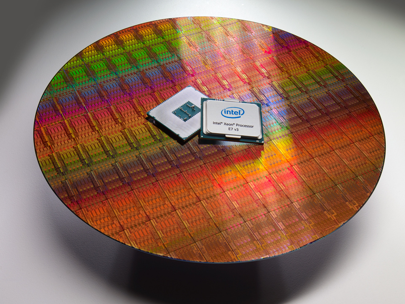
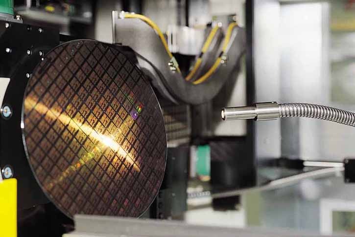
An example of a wafer used to produce Intel's Xeon E7 processor in 2015, which uses photolithography in its creation, with the finished processor itself for scale.
While established, the technique has its problems, such as modern chips needing more than 50 different mask passes as part of its production, with the higher number of masks increasing the possibility of a manufacturing flaw, and in turn wasting the expensive wafer. There is also the limitation from the use of a laser as a light source, as current practicable versions work at too long a wavelength for it to be practicable at extremely small sizes that processor production now calls for.
To work around this, companies are now looking towards ways to refine the well-worn process for smaller and more complex dies.
Extreme Ultraviolet Lithography
The technique of Extreme Ultraviolet Lithography (EUL) is seen to be the key to future die shrinks, with the technique relying on a completely different light source. While still using a laser, it is in fact used to excite tin or xenon plasma under vacuum to provide light at a wavelength of 13.5 nanometers, far lower than the 193nm-or-more wavelengths used in the above process.
This means that the light can be used with masks to provide a far higher potential resolution for chip production than previously possible. It may also offer other benefits, with Samsung suggesting in late 2018 that the process could use only one multi-patterning mask to develop one layer rather than four previously required, reducing the number of masks and production steps required.
While promising, EUL has so far yet to make it into commercial chip production lines in a significant way. The long development process of the technique still has its challenges that companies have to straighten out, as with any new processes that are just entering commercialization, but the performance rewards and potential cost savings from using it at scale are worth chasing by all involved.
Intel — 14-nanometer, still
Intel first released chips using its 14-nanometer process in 2014, and has largely spent the time since then refining the process and maximizing its investment. Even chips it launched in April 2019 used the 14-nanometer process instead of something newer.
When Intel introduced the 14-nanometer process, its main change from the 22-nanometer version was its second generation of "tri-gate transistors," a three-dimensional transistor design that used a raised drain "fin" rather than using a two-dimensional planar transistor structure. The iteration introduced with the 14-nanometer process reduced the cost and power required per transistor, as well as increasing the density, making it more cost effective to produce and higher performance.
Since 14-nanometer's introduction, Intel has been working on commercializing a 10-nanometer process, but it has struggled to do so with reports of low chip yields. Until the process was cost-effective enough, and didn't waste too much of each wafer, it was repeatedly delayed from launch, at one point causing Intel to deny claims it had abandoned the seemingly doomed fabrication process altogether.

Ice Lake, Intel's first proper crack at commercializing 10-nanometer processes
In May, Intel claimed it would commence shipments of a 10-nanometer processor in June, part of the "Ice Lake" generation.
Intel does harbor ambitions to go smaller, advising at the same time to investors it was planning on finishing work on a die shrink to a 7-nanometer process in the coming years. The first release using the process, which is tipped to use EUL, will be the Intel Xe "general-purpose GPU" for high performance computing and data center AI applications, possibly arriving sometime in 2021.
TSMC — 7-nanometer and limboing further
TSMC is best known for being the foundry that produces Apple's A-series chips that are used in iOS devices, with the latest model of iPhone accompanied by the latest release in the series. The last few have been made using a 7-nanometer process, which TSMC achieves using the same sort of photolithography techniques as the rest of the industry.
Even TSMC is keen to move on with EUL for its products, even for the current 7-nanometer level. In April, it was reported the firm was leveraging EUL for its "N7+ process," with a further refinement dubbed "N7 Pro" thought to be intended for use with the 2019 A-series release.
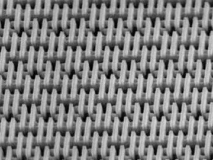
A close-up image of TSMC's 7nm Fin Field-Effect (FinFET) process
The next major process TSMC will use is "N6," which will be a 6-nanometer version that again uses EUL, and stands to offer an 18-percent greater logic density than designs made under N7. Risk production of the process will start in the first quarter of 2020, ahead of its potential usage in the 2020 iPhone refresh.
Going even smaller, TSMC is already planning for 5-nanometer chips by completing the design infrastructure for the process and providing it to key customers, so they can adopt their plans to use the process. Standing to offer 1.8 times the logic density and a 15-percent speed gain over 7-nanometer equivalents, the 5-nanometer process is also said to be close to entering risk production, which may make it a second TSMC candidate process for the 2020 iPhone's A-series chips.
So, what's really different?
While Intel and TSMC are effectively using the same fundamental techniques for processor production, there isn't any obvious explanation for why one is sticking at 14nm and the other thriving at 7nm. As firms dealing with billions of dollars worth of budgeting decisions, they are obviously quite secretive about their particular processes, making finding a reason why there is such a disparity a tricky one.
Intel's "low yield" commentary in defending its glacial development of the 10-nanometer process is the nearest that we will get to an explanation. While it is expected there will be some loss in production when producing many chips on a wafer at such a small level using a laser with a wavelength in the hundreds of nanometers, sometimes the amount of loss from production is too great to continue with.
Moving down to a smaller process, the chance of a failed chip being produced increases, but at the same time the space the chip takes up reduces.
In the case of comparing 14-nanometer with 7-nanometer processes, the latter could potentially create four chips in the space one chip for the former process occupies. If the cost of applying processes is the same, so long as the chance of failure doesn't scale up too far, the increase in lost chip production can still be offset enough to make it more profitable.
With the perfection of EUL, this may become less of a problem as the industry tries to make even smaller processes, but until that point, it may simply be a question of economics.
To confuse matters further, there isn't any industry standard way of officially defining what size a process actually is, and how each company implements each scaled down process can also play a factor. While a 14-nanometer chip from one producer may seem less impressive than one declared to be using a recently-commercialized 10-nanometer process by another company, it is entirely plausible the performance of the two could be comparable, depending on the implementation of each.
With this disparity, this can effectively turn that nanometer figure into a feature for marketing. Even if it performs at a similar level to chips using a slightly larger process, just being able to say the smaller process is being used can hype one chip over another, despite there being no real extra benefit to end users.
There is also little accuracy in declaring one company to be better than the other based on nanometers. Sure, Intel is only just getting to 10 nanometers while TSMC has been at 7 nanometers for a while, but a direct comparison just cannot be made.
The density of transistors you can squeeze into a small space is not the ultimate metric for performance. The designs, the features you put into a chip, and the ones you leave behind as the chip iterates — these all have just as much of a bearing on performance as a die shrink.
To customers, the difference between processes is a moot point. Features like the number of cores and clock speeds on a processor in a Mac may be worth knowing about more than whether the chip was made using a 14-nanometer or 10-nanometer process.
For mobile devices like the iPhone, it matters even less. Is it the fastest A-series chip Apple has ever designed inside the latest model of iPhone? Yes it is, and really, that's all that matters.