Apple's imminent M5 Pro and M5 Max chips will run cooler and faster than ever before, as a year-old rumor about the way Apple Silicon chips are packaged resurfaces.
Apple is anticipated to bring out the M5 Pro and M5 Max chips as part of a MacBook Pro update in early 2026. However, while performance improvements are expected for the higher-tier chips, the way they are produced will make as much of an impact as improving clock speeds and core counts.
In a February 3 Weibo post, serial leaker Fixed Focus Digital added more context to a comment they made a few days earlier, on January 31. At that time, they said that the upper M5 chips will use TSMC's SoIC packaging, which had also reduced in cost to perform.
In the February follow-up, the leaker says that there will be obvious heat dissipation and low resistance advantages. The change will still be a "2.5D package," with a higher density than that of "InFo."
In short, the inbound chips will be able to run faster because of the packaging, while also being able to run cooler, minimizing throttling.
While Weibo leakers don't have a good reputation when it comes to accuracy, Fixed Focus Digital has a relatively mixed track record, with some claims proving to be true. However, previous rumors on this topic work in their favor in this instance.
Better packaging
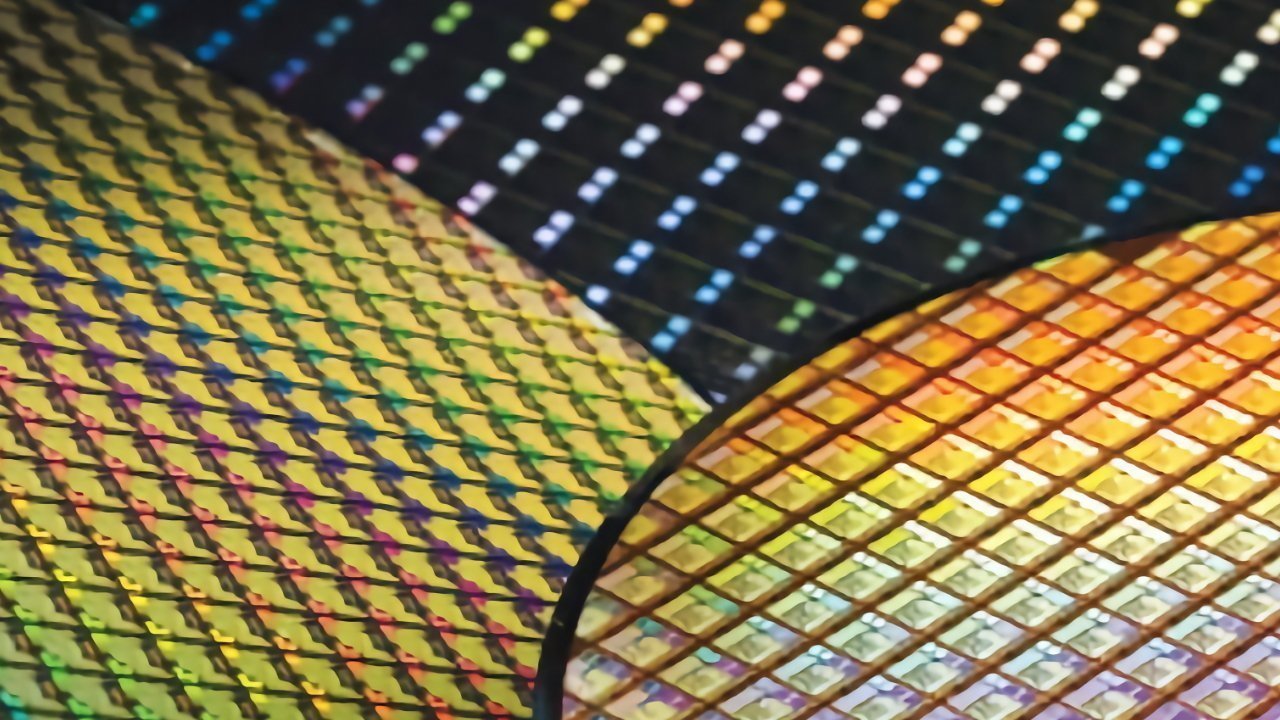
The discussion here is about chip packaging, namely a process applied to the chip's die. It is a crucial element, determining how the chip communicates with other components.
InFo, or Integrated Fan-Out, is the current method used to create very compact chips, such as those used for the iPhone. Its size is certainly beneficial for creating slimline devices, but it is one that is typically used with a single die instead of multi-die operations.
This is great for efficiency and size, but the use of a single large die can cause thermal problems that results in throttling.
SoIC, on the other hand, refers to TSMC's System on Integrated Chips technique. It's a 3D chip-stacking process, which layers smaller chip sections on top of each other to create the larger chip.
When Fixed Focus Digital refers to this as a "2.5D package," this means that the smaller dies are combined side-by-side on a common interposer. This is a bridge technique between the vertically-stacked 3D and spread out 3D techniques.
The technique is one that offers benefits from both worlds. There are performance improvements from having closely-connected dies from 3D packaging, but with the ability to thermally manage the package closer to a thin 2D process.
A major flexibility change
To consumers, the way the chip is packaged can have a lot more of a bearing on how the chip works, beyond general performance and thermal improvements.
By using multiple small dies, there is an opening for Apple to be more flexible with its designs. As previously proposed by Ming-Chi Kuo in late 2024, Apple could have separate chiplets for the CPU and GPU, so they can be combined in different ways.
Instead of baking a CPU and GPU combination into a single die, TSMC could instead create separate CPU and GPU dies, which are put together in the packaging process in specific configurations.
For consumers, this could mean more choice in terms of CPU and GPU combinations.
For Apple, it will mean a much cheaper way of making chips while still offering variety.
The base cost-saving is in splitting up the die into multiple parts. As each CPU and GPU element can be made separately, there should be much higher yields post-packaging than combining them all onto one die.
This will reduce overall wastage in production compared to higher single-die failure rates, as well as potentially cutting down on acts of chip binning.
At a time when memory prices are skyrocketing, it's a much-needed cost-saving measure, especially when the demand for chips is extremely high.